What Circuit Board Layouts in High-Speed Motherboards Reveal About Maintaining Signal Stability During Sustained 8K Gaming Workloads
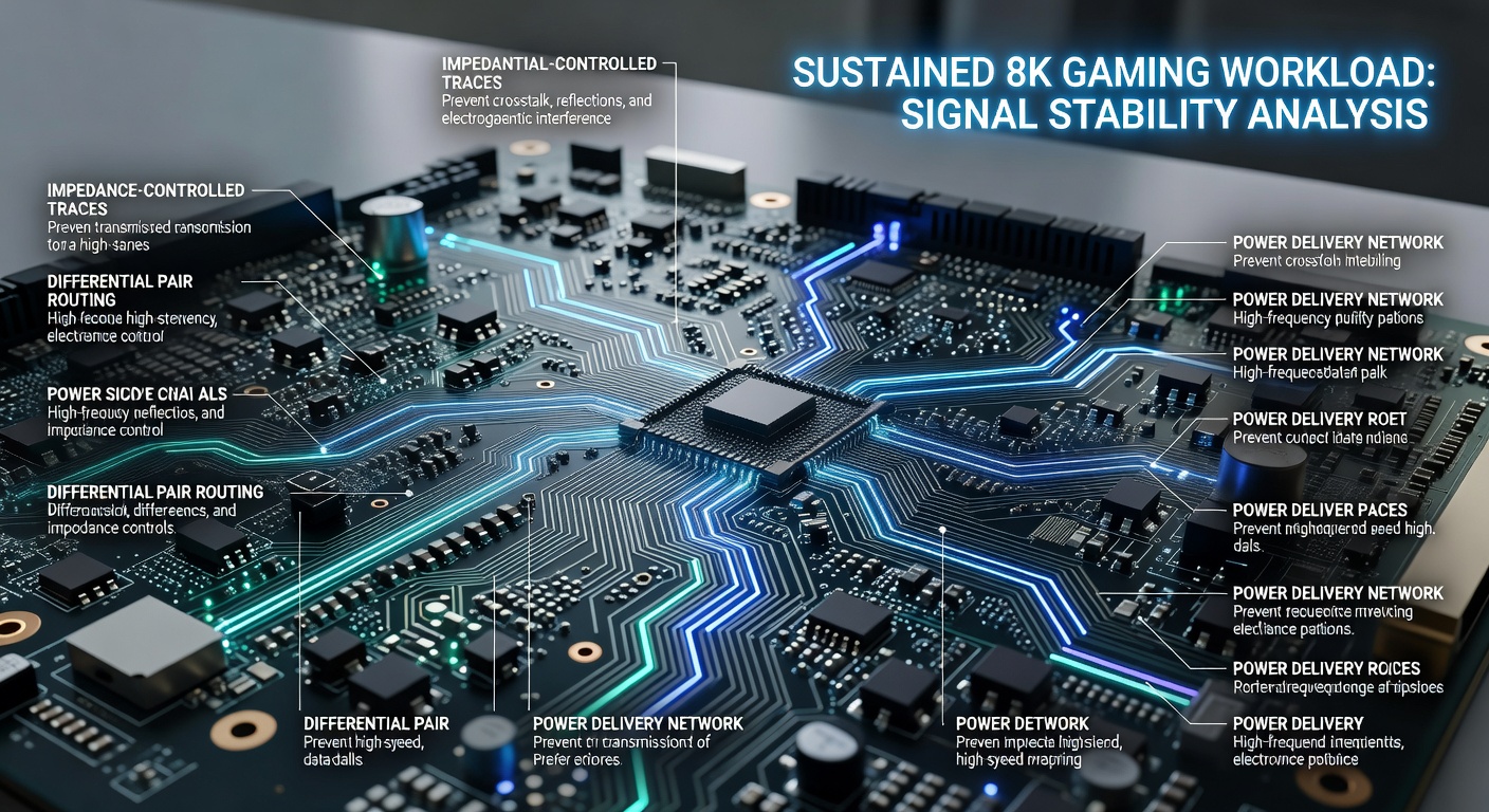
High-speed motherboards designed for 8K gaming must handle enormous data rates across multiple interfaces, and circuit board layouts play a central role in preserving signal integrity under continuous loads that push components to their limits. Engineers arrange traces, planes, and vias with precise attention to impedance matching, differential pair routing, and return path continuity so that signals traveling between CPU, GPU, and memory subsystems remain stable even after hours of operation.
Studies from research institutions show that impedance discontinuities become pronounced when trace lengths exceed certain thresholds at frequencies required for 8K content delivery. Controlled dielectric materials combined with consistent trace widths keep characteristic impedance within tight tolerances, which reduces reflections that could otherwise corrupt data packets during extended sessions. Observers note that manufacturers now incorporate more layers in stack-ups, often reaching twelve or fourteen copper planes, to separate high-speed signals from power delivery networks and thereby minimize crosstalk.
Trace Routing and Differential Pair Strategies
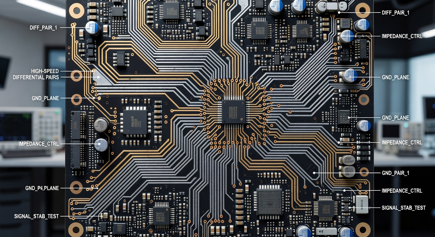
Routing differential pairs for PCIe lanes and memory channels requires equal lengths within a few mils while maintaining consistent spacing to preserve coupling. Engineers use serpentine patterns when necessary to equalize paths, yet they avoid sharp bends that create impedance spikes. Ground planes placed directly beneath these pairs provide clean return currents, and stitching vias connect reference planes at regular intervals to prevent slot antenna effects that radiate noise under sustained workloads.
Data from industry reports indicate that 8K gaming stresses memory controllers continuously, with data rates pushing toward 8000 MT/s and beyond in 2026 configurations. Layouts that interleave power and ground planes help suppress simultaneous switching noise, which grows when multiple DRAM ranks activate in rapid succession. Researchers at technical universities have measured eye diagrams on test boards showing that optimized via transitions and back-drilling reduce stub resonances that degrade margins at these speeds.
Power Delivery Networks and Thermal Considerations
Stable voltage rails matter because fluctuating power delivery can modulate signal levels and introduce jitter. Wide copper pours and multiple parallel planes lower DC resistance and inductance, allowing current spikes from GPUs rendering 8K frames to pass without significant voltage droop. Decoupling capacitors placed close to load points, combined with careful plane segmentation, maintain low impedance across the frequency spectrum encountered during long gaming sessions.
Thermal expansion during prolonged operation affects trace geometry slightly, and high-end designs account for this by selecting materials with matched coefficients of thermal expansion. As of May 2026, several motherboard vendors publish layout guidelines that include thermal simulations showing how localized heating near voltage regulators can influence nearby high-speed traces if not isolated properly.
Testing and Validation Practices
Validation teams rely on time-domain reflectometry and vector network analyzers to verify that fabricated boards match simulation models. Bit error rate tests under full 8K workloads reveal whether layout choices keep margins acceptable after temperature cycling. One study conducted across multiple board revisions demonstrated that adding more ground stitching vias around critical connectors reduced electromagnetic interference by measurable amounts during continuous operation.
Industry organizations such as the IEEE have published standards that guide these practices, emphasizing the importance of consistent reference planes and minimized via stubs. Engineers also examine manufacturing tolerances because even small deviations in dielectric thickness or copper etch can shift impedance enough to affect stability at multi-gigahertz frequencies.
Emerging Layout Techniques
Advanced techniques now include embedded traces and low-loss laminates that support higher frequencies with less attenuation. Some designs route sensitive signals on inner layers surrounded by ground planes on both sides, shielding them from external noise sources while maintaining mechanical rigidity. Observers point out that these approaches become essential when motherboards incorporate multiple high-bandwidth expansion slots that operate simultaneously during demanding titles.
Power integrity analysis often runs in parallel with signal integrity checks because the two domains interact through shared return paths. Simulations that model both simultaneously help identify regions where current loops might couple into signal traces and create timing errors over long sessions. Manufacturers refine these layouts iteratively using feedback from real-world stress testing that replicates sustained 8K rendering conditions.
Conclusion
Circuit board layouts in high-speed motherboards encode critical lessons about preserving signal stability when systems endure extended 8K gaming demands. Precise impedance control, thoughtful plane allocation, and rigorous validation together enable reliable performance under continuous stress. As hardware evolves, these foundational layout principles continue to guide development toward even higher data rates and longer operational durations.