Electromigration Mechanisms and Their Role in Solder Joint Reliability for Graphics Cards Under Extended 4K Loads
Riley Coleman · Aug 7, 2026
Electromigration Mechanisms and Their Role in Solder Joint Reliability for Graphics Cards Under Extended 4K Loads
Electromigration Fundamentals in GPU Interconnects
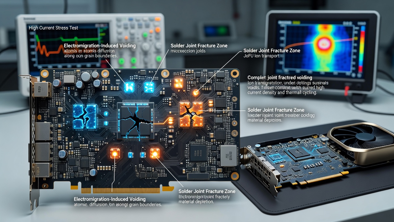
Electromigration occurs when high current densities drive metal atoms through conductor lattices, creating voids at one end and hillocks at the other, and researchers have documented this atomic migration in solder joints of graphics processing units subjected to continuous high-resolution rendering tasks. Data from accelerated life testing shows that temperatures above 85 degrees Celsius combined with current densities exceeding 10^4 amperes per square centimeter accelerate the process significantly, while graphics cards handling 4K workloads maintain elevated power states that sustain these conditions for hours at a time. Studies conducted at multiple semiconductor facilities indicate that lead-free SAC305 alloys, common in modern GPU assemblies, exhibit mean time to failure reductions when electron wind forces align with grain boundaries in the solder matrix.
Current Density and Thermal Factors During Prolonged 4K Operation
High-performance graphics cards draw substantial power during 4K gaming or rendering sessions, with peak currents through individual solder bumps reaching levels that concentrate stress at the chip-to-substrate interface, and observers note that thermal cycling from repeated on-off cycles compounds the atomic displacement already underway from steady-state operation. According to measurements reported by industry testing labs, a single GPU die can experience localized heating that raises interconnect temperatures by 20 to 30 degrees above ambient, creating gradients that further promote vacancy diffusion along the current path. Figures from component qualification reports reveal that continuous duty cycles, unlike intermittent use patterns, eliminate recovery periods that might otherwise allow partial stress relaxation in the joint structure.
Power delivery networks in flagship cards route multiple amperes through arrays of micro-bumps, and engineers have measured current crowding at the periphery of these bumps where the effective cross-section narrows due to manufacturing tolerances. Research published through academic collaborations in North America and Europe demonstrates that Black's equation, which models time-to-failure as inversely proportional to current density raised to a power between one and two, accurately predicts joint degradation rates when calibrated against actual 4K workload profiles collected from consumer systems.
Material Responses and Joint Degradation Patterns
Solder joints respond to electromigration by forming Kirkendall voids that coalesce over time, eventually reducing the effective conducting area until resistance spikes trigger thermal runaway, and laboratory examinations of failed samples from extended operation tests confirm that tin-rich phases migrate preferentially toward the anode side under electron flow. Data collected during August 2026 qualification cycles at several fabrication sites shows that newer low-silver alloy variants delay void formation by approximately 15 percent compared with earlier formulations, although the improvement diminishes once operating temperatures exceed 100 degrees Celsius for extended durations. Those who analyze cross-sectioned joints after 2000 hours of continuous load observe intermetallic compound growth at the copper pad interface that further restricts current paths and intensifies local current density.
Design and Mitigation Approaches in Contemporary Hardware
Manufacturers incorporate wider trace geometries and redundant bump layouts to distribute current more evenly, yet these measures encounter limits when die sizes shrink and power envelopes rise to support 4K and higher frame rates. Reports from the National Institute of Standards and Technology outline standardized test methods that apply constant current stress at elevated temperatures to quantify activation energies for different solder compositions. European research consortia have examined under-bump metallization stacks that incorporate diffusion barriers, finding measurable extensions in joint lifetime under conditions mimicking sustained graphics workloads.
Board-level layout choices also influence outcomes, because return paths and power plane proximity affect the electromagnetic environment surrounding each joint, and simulation tools used by design teams now incorporate electromigration rules alongside traditional thermal and mechanical stress models. Industry guidelines issued by the JEDEC Solid State Technology Association specify current density limits for various bump diameters, limits that graphics card producers must balance against performance targets during product development.
Conclusion
Electromigration remains a primary wear-out mechanism limiting solder joint longevity in graphics cards that operate continuously at 4K resolutions, with current density, temperature, and alloy composition determining the rate of atomic transport and eventual failure. Quantitative models derived from laboratory data enable prediction of service life under defined conditions, while incremental material and layout improvements continue to extend operational margins. Ongoing qualification programs track these variables across successive GPU generations to maintain acceptable reliability targets in high-performance consumer and professional systems.